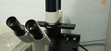
High Resolution Transmission Electron Microscope (HRTEM) with EDAX

Instrument specification
JEOL 3010 with a UHR polepiece operates at an accelerating voltage 300 kV. Depending upon the sample compatibility, it can work at three different accelerating voltages i.e., 300, 200 and 100 kV. This has a filament made up of LaB6. The instrument works under a vacuum in the range 10-5 to 10-6 Pa. This gives a lattice resolution of 0.14 nm and a point-to-point resolution of 0.12 nm. It is fitted with an ultra-high resolution pole piece (Cs=0.6mm). Images are collected using a Gatan Orius SC200 CCD camera (2K x 2K) with a Windows XP computer running Digital Micrograph software. This camera is capable of recoding in-situ events at TV rate as well as high resolution images.
Technicalities
HRTEM is an instrument for high-magnification studies of nanomaterials. High resolution makes it perfect for imaging materials on the atomic scale. A main advantage of a TEM over other microscopes is that it can simultaneously give information in real space (in the imaging mode) and reciprocal space (in the diffraction mode). Our instrument has a single tilt stage and maximum Tilt Angle of -10° to +10° in Goniometer. The instrument can operate in Bright-Field, Dark-Field, High resolution, SAED and CBED modes. We have a standard probe and a variable temperature probe
(100 to 500 K). TEM is coupled with a Gatan digital camera for digital image processing. The instrument can go upto a maximum magnification of 1.5 million. It has an ACD (anti contamination device) working with the aid of liquid nitrogen, which helps the filament from contamination caused by volatile sample.
Key features of HRTEM technology
- Resolution: 0.14 nm lattice, 0.12 nm point-to-point.
- Accelerating Voltage: 100, 150, 200, 250, 300 kV.
- Filament: Pre-centred LaB6.
- Objective lens: focal length 2.5mm, Cs 0.6mm, Cc 1.3mm, minimum focus step 1nm.
- Spot Size: TEM mode 200~20nm dia (5 steps), EDS/NBD/CBD mode 25~1.0nm (8 steps).
- Magnification Range: 4,000x – 1,5000,000x.
- High dispersion diffraction camera length range: 4 to 80 m.
- Specimen Tilt range: +/-20 degrees (for UHR configuration), +/-30 degrees (for HR and HC configuration).
Schematic of the JEOL 3010 instrument*

For more information on the instrument visit Transmission electron microscopy – Wikipedia.
Theory of operation
Basic principle of TEM is quite similar to their optical counterparts, the optical microscope. The major difference is that in TEM, a focused beam of electrons instead of light is used to “image" and achieve information about the structure and composition of the specimen. An electron source usually named as the “Gun” produces a stream of electrons which is accelerated towards the specimen using a positive electrical potential. This stream is then focused using metal apertures and magnetic lenses called “condenser lenses” into a thin, focused, monochromatic beam. Beam strikes the specimen and a part of it gets transmitted through it. This portion of the beam is again focused using a set of lenses called “objective lenses” into an image. This image is then fed down the column through the “intermediate and projector lenses”, which enlarges the image, depending upon the set magnification. A phosphor image screen is used to produce the image. The image strikes screen and light is engendered, which enables the user to see the image. The darker areas of the image represent the thicker or denser region of the sample (fewer electrons were transmitted) and the lighter areas of the image represent those areas which are thinner or less dense (more electrons were transmitted.
Notable mentions

References
- Ambient microdroplet annealing of nanoparticles, Angshuman Ray Chowdhuri, B. K. Spoorthi, Biswajit Mondal, Paulami Bose, Sandeep Bose and Thalappil Pradeep, Chem. Sci., 12 (2021) 6370–6377 (DOI: 10.1039/d1sc00112d).
- Atom transfer between precision nanoclusters and polydispersed nanoparticles: A facile route for monodispersed alloy nanoparticles and their superstructures, Paulami Bose, Papri Chakraborty, Jyoti Sarita Mohanty, Nonappa, Angshuman Ray Chowdhuri, Esma Khatun, Tripti Ahuja, Ananthu Mahendranath and Thalappil Pradeep, Nanoscale, 12 (2020) 22116-22128 (DOI: 10.1039/D0NR04033A).
- Atomically precise nanocluster assemblies encapsulating plasmonic gold nanorods, Amrita Chakraborty, Ann Candice Fernandez, Anirban Som, Biswajit Mondal, Ganapati Natarajan, Ganesan Paramasivam, Tanja Lahtinen, Hannu Häkkinen, Nonappa, Thalappil Pradeep, Angew. Chem. Int. Ed., 57 (2018) 6522–6526 (DOI: 10.1002/anie.201802420).
- Holey MoS2 nanosheets with photocatalytic metal rich edges by ambient electrospray deposition for solar water disinfection, Depanjan Sarkar, Biswajit Mondal, Anirban Som, Swathy Jakka Ravindran, Sourav Kanti Jana, C. K. Manju and Thalappil Pradeep, Global Challenges, (2018) 1800052 (DOI: 10.1002/gch2.201800052).
- Unusual reactivity of MoS2 nanosheets, Biswajit Mondal, Anirban Som, Indranath Chakraborty, Ananya Baksi, Depanjan Sarkar and Thalappil Pradeep, Nanoscale, 8 (2016) 10282–10290 (DOI: 10.1039/c6nr00878j).
- Cluster mediated crossed bilayer precision assemblies of 1D nanowires, Anirban Som, Indranath Chakraborty, Tuhina Adit Maark, Shridevi Bhat and Thalappil Pradeep, Adv. Mater., 28 (2016) 2827-2833 (DOI: 10.1002/adma.201505775).
- Metallic nanobrushes made using ambient droplet sprays, Depanjan Sarkar, M. K. Mahitha, Anirban Som, Anyin Li, Michael Wleklinski, R. G. Cooks and Thalappil Pradeep, Adv. Mater., 28 (2016) 2223–2228 (DOI: 10.1002/adma.201505127).
- Anisotropic molecular ionization at 1 V from tellurium nanowires (Te NWs), Rahul Narayanan, Depanjan Sarkar, Anirban Som, Michael Wleklinski, R. G. Cooks and Thalappil Pradeep, Anal. Chem., 87 (2015) 10792-10798 (DOI: 10.1021/acs.analchem.5b01596).
- Manifestation of the difference in reactivity of silver clusters in contrast to its ions and nanoparticles: The growth of metal tipped Te nanowires, Anirban Som, Akshaya Kumar Samal, Thumu Udayabhaskararao, M. S. Bootharaju and Thalappil Pradeep, Chem. Mater., 26 (2014) 3049−3056 (DOI: 10.1021/cm403288w).
 Search
 Sign in


 Total views : 240731